Home | Focus |Program |Photos |Scientific committee |Abstracts | Travel |Registration |Past Meetings
![]()
Oligofunctional DNA-Au Nanoparticles for the Assembly of Particle Layers B. Ceyhan 1 , P. Hazarika 1 , M. Noyong 2 , U. Simon 2 and C.M. Niemeyer 1 1 Biologisch-Chemische Mikrostrukturtechnik, Universität Dortmund, Germany DNA has become a useful tool for controlled assembly of metal and semiconductor nanoparticles. We here report on oligofunctional gold nanoparticle conjugates containing different DNA sequences (Dn-Au in Fig 1).[1] The index in Dn-Au denotes the number of different sequences attached to the nanoparticle, ranging from one (monofunctional) up to seven (heptafunctional). The individual oligomers of Dn-Au are orthogonally addressable and reveal an efficient reactivity which is comparable to that of the analogous monofunctional conjugates. We also report the two dimensional assembly of difunctional gold nanoparticles containing two different DNA sequences.[2] One sequence is used for the selective immobilization on the substrate, the other one interconnects the particles. The samples are analyzed by AFM and UV/VIS measurements. The monolayer assemblies partially reveal hexagonally ordered arrays. Schematic drawing of a heptafunctional gold nanoparticle conjugate (a). Scheme (b) and AFM image (c) of two dimensional gold nanoparticle aggregates, immobilized and cross-linked via two different DNA sequences. 1. C.M. Niemeyer, B. Ceyhan, P. Hazarika, Angew. Chem. Int. Ed. 42 (2003), 5766-5770. A toolbox for molecular construction based on DNA, metal nanoparticles and microstructured surfaces Andrea Csaki, Gunter Maubach, Detlef Born, Andrea Steinbrück, Andreas Wolff, Wolfgang Fritzsche Institute for Physical High Technology Jena, Germany The construction of novel nanoscale materials and devices using molecular units offers a large potential for future technologies. We present here our system aiming at basic operations in molecular construction, combining the versatile DNA-nanoparticle conjugates with long DNA precisely positioned at microstructured surfaces.The inclusion of metallization techniques both based on direct metallization and nanoparticle-mediated techniques has been studied. Another interesting problem is a step-wise extension of DNA by partial hybridization. Using nanoparticle labeling, the efficiency of substrate-based constructs was compared with constructs pre-assembled in solution. A. Csaki, P. Kaplanek, R. Möller and W. Fritzsche: Single particle sensitivity in the optical detection of individual DNA-conjugated nanoparticle after metal enhancement. Nanotechnology 14 (2003), 1262-1268. Theoretical investigation of metal-containing DNA-based helices R. Di Felice 1 , A. Calzolari 1 , H. Zhang 1 , A. Garbesi 2 , E. Molinari 1,3 1 National Research Center on nanoStructures and bioSystems at Surfaces (S3), Modena, Italy Recent efforts in the field of molecular electronics are being extended to the use of biomolecules for device fabrication. The advantages of using biomolecules, rather than more conventional organic molecules such as conducting polymers and others, are linked to their intrinsic functionality (e.g., electron-transfer metalloproteins) and unique structuring. For instance, by virtue of their recognition and self-assembling properties, DNA molecules seem particularly interesting in this framework. However, whereas double-stranded DNA has been successfully employed as a template for metallic wires [1], its performance as a conductor is still questioned and several data indicate that native DNA attached to inorganic substrates is an insulator [2].Despite this evidence, it would be very appealing to combine the structural properties of DNA with an intrinsic molecular conductivity without destroying recognition. To this aim, ongoing investigations are focusing on the search of novel modified DNA molecules that would have suitable electronic properties [3]. [1] E. Braun, Y. Eichen, U. Sivan, and G. Ben-Yoseph, Nature 391, 775 (1998). Enabling methods for nucleic acid and nanoparticle-based molecular electronics August Estabrook 1 , Norbert Reich 1 , Gary Braun 1 , Inagaki Katsuhiko 2 , Andrew Cleland 2 , Geoff Strouse 3 1 Department of Chemistry and Biochemistry, University of California, Santa Barbara, CA. We are developing methods for the robust assembly of nucleoprotein and nanoparticle-based molecular electronics. Current non-specific deposition methods (Ag and Au on DNA) result in 50-100 nanometer "wires", which are relatively large for molecular electronics. We have assembled positively charged 4-13 nanometer gold nanoparticles on 300-4000 base pair DNA elements attached via 5' thiol linkages to nanoelectrodes and used these for conductance measurements. We are also developing novel molecular biological methods to create 20 nucleotide overhangs on 300-4000 base pair DNA elements for directed assembly, both in electrodes and on non-mobile cruciforms; this approach is similar to recent uses of lambda DNA, but is more versatile. We have designed multi-targeting zinc finger proteins to act as molecular interconnects between our DNA elements; this approach should have broad use in the nucleic acid based approach to molecular electronics. 1. 4000 bp DNA segment treated with positively charged 4 nanometer nanoparticles. 2. AFM of 13 nm Au appended to each end of a 600 bp PCR fragment via C6 thiol linkers. Dimensions in microns. 3. A, Cruciform design and analysis. B, design and analysis of cruciform with 300 bp arms. C, 5' hexyl thio linkage for attachment to gold surface and nanoparticle. Non-covalent binding of DNA to carbon nanotubes controlled by biological recognition complex Laurence Goux-Capes 1,3 , Arianna Filoramo 3 , Denis Cote 2 , Jean-Philippe Bourgoin 1 and Jean-Nöel Patillon 3 1 Laboratoire d'Electronique Moléculaire, CEA Saclay, DSM/DRECAM/SCM, 91191 Gif-sur-Yvette, France Single wall carbon nanotubes (SWNTs) occupy a special place within molecular electronics. Indeed, they exist as semiconducting or metallic wires and have been used to demonstrate molecular devices like transistors, diodes or SET (single electron transistor). However, the future of this class of SWNT-based devices is to a large extent related to the development of a bottom-up self-assembly technique. The exceptional recognition properties of DNA molecule make it an ideal candidate for this task. Here, we describe a non-covalent method to connect carbon nanotubes to DNA strands using the streptavidin/biotin complex. Control experiments show that in absence of biotin, the DNA strand do not bind to SWNT. Moreover, these DNA-SWNTs complexes have been combined with molecular combing (see as example figure 1) and/or self-assembled monolayers (SAMs) techniques to go towards bottom-up self-assembled carbon nanotubes arrays. Molecular combing of DNA-NT complex A parallel approach to DNA nanotechnology: Step-by-step self assembly of metal nanostructures in microelectrode arrangements using a DNA template Wolfgang Fritzsche, Gunter Maubach, Andrea Csaki, Detlef Born Institute for Physical High Technology Jena, Germany Molecular self assembly based on specific binding pairs is a promising approach in DNA-based nanoelectronics. However, to transform these experiments into a technology, an integration with todays technical platforms is required. This integration is usually realized by low-yield random adsorption onto prestructured electrode arrangements or by physical nanotechniques, such as e-beam lithography or conductive AFM. These serial approaches are time-consuming and limit the number of possible experiments. Comparative imaging of the same DNA structure spanning a microelectrode gap by fluorescence microscopy (left), AFM (center) and SEM (after nanoparticle labeling) [3] 1. Fritzsche, W.; Maubach, G.; Born, D.; Köhler, J. M.; Csaki, A. (2002) in DNA-Based Molecular Construction pp 83-92, AIP Conference Proceedings Vol. 640. Charge transfer and oxidative damage in DNA fibers Francesco Gervasio Chemical Physics, ETH Zuerich c/o USI campus, Lugano, CH Recently there has been great interest in the nature of the electronic structure of DNA because of its potential applications to nanotechnology. Indeed DNA has several properties that make it attractive in a variety of applications. It is a stable polymer and can easily be handled and modified almost at will. Furthermore, its one-dimensional character and regular stacking of pi-bases have suggested the possibility of using DNA as a nanoscale conductor. Unfortunately, experiments have provided very contradictory results. Theory could be of great help in understanding these phenomena provided that all the important constituents of this complex molecule are taken into account (i.e. charged sugar-phosphate backbone, solvating water and counter-ions). Using state of the art ab-initio simulation we investigated a laboratory realizable wet DNA molecule in the radical cation state. We studied the localization of the hole, possible mechanisms of charge transfer and the guanine oxidation, which is important as a parasite event that stops charge transfer but also from a biological point of view as the first step in DNA oxidation, a common event that in absence of repairing mechanisms eventually leads to fatal consequences as cancer and mutagenesis. Chemistry at a distance: Electron transport through DNA Bernd Giese Department of Chemistry, University of Basel, Switzerland Electron transport through DNA and peptides occur via the heterocyclic bases and aromatic side chains of these biopolymers. There are numerous biological applications. Thus photolesions of DNA are repaired in an electron-catalyzed reaction[1]. Transport of an electron from a remote thymine radical anion through DNA occurs in a multistep hopping process. When the electron meets a thymine dimer, which is generated by photocycloadditon of adjacent thymine residues, the two thymine bases are repaired through a retro-cycloaddition reaction, while the electron continues along the DNA. AFM based techniques to measure conductivity in DNA based Nanowires Julio Gomez Universidad Autonoma de Madrid, Spain In this talk we will present different atomic force microscopy (AFM) based techniques developed by our group to characterise the electrical properties of DNA based nanowires. Towards Deterministic Bottom-up Assembly of Metal Nanoparticles Marcus R. Helfrich, Lisa M. Dillenback, Rebecca L. Stoermer and Christine D. Keating Department of Chemistry, Penn State University, University Park, PA 16802 USA This presentation will discuss current efforts towards the bottom-up assembly of metal nanoparticles into predetermined, functional architectures. DNA hybridization is used as a highly selective "glue" to bind nanospheres or nanowires together. In addition to the selectivity of Watson-Crick base pairing, we are confining the assembly process to two dimensions at an aqueous-aqueous interface and are controlling the temporal sequence of assembly events through hybridization temperature/sequence. Special challenges inherent in assembly at the aqueous-aqueous interface will be addressed. Striped nanowires offer several opportunities as building blocks; their length, width, and composition can be controlled as desired, for example to tailor electrical properties. Specific assembly targets include function blocks for integration into molecular electronic memory and logic devices. Electric Field Based Process for Producing Linear Electronic/Photonic Transfer Nanostructures Michael J. Heller Departments of Bioengineering/Electrical and Computer Engineering, University California San Diego, La Jolla, CA 92093 Active microelectronic arrays which have been developed for genomic research and DNA diagnostic applications may also have potential for nanofabrication applications. These microarray devices are able to create reconfigurable electric field transport geometries on their surface which allows charged reagent and analyte molecules (DNA, RNA, oligonucleotide probes, amplicons antibodies, proteins, enzymes, nanoparticles and micron sized semiconductor devices) to be moved to or from any of the microscopic test sites on the device surface. These microelectronic array devices have the potential for many nanofabrication applications, including the directed self-assembly of molecular, nanoscale and microscale components into more complex structures and for creating higher-order mechanisms. This type of electric field assisted self-assembly using active microelectronic arrays is being investigated as a method to carry out the selective functionalization of nanocomponents with high precision. Present nanofabrication methods do not allow most nanostructures (quantum dot, photonic crystal, fluorescent polymer nanoparticles, metal and ceramic nanoparticles, etc.) to be modified in a controlled or precise manner. While such processes do allow a higher-order nanostructure to be formed, there is little or no control as to how the functional groups (chemical ligands, proteins, DNA, etc.) are arranged around the core nanostructure. Furthermore, it is very difficult to arrange "different" binding entities around the core structures. We are developing technology that will allow core nanostructures to be modified as show in Figure A. In this case, the nanocomponents can be derivatized at specific positions around the core with specific DNA (oligonucleotides), proteins, or other biological or chemical entities. Such modifications will allow different nanocomponents to be assembled in a more precise manner, and to create more heterogeneous higher-order nanostructures as shown in Figure B. Formation and electrical properties of DNA-immobilized gold nanoparticle monolayers E. Hesse, U. Simon RWTH Aachen, Institute of Inorganic Chemistry, Aachen, Germany Self-organization of metal nanoparticles into well defined assemblies is of tremendous interest particularly with regard to the electronic properties of these systems.Owing to its unique recognition capabilities, DNA can be used as a molecular linker for gold nanoparticles and is a promising construction material for their precise spatial positioning [1].The site-selective immobilization of gold nanoparticles functionalized with DNA oligomers onto gold substrates is well established in our working group [1,2] but the metallic substrates inhibit the examination of the electronic properties of these systems. Therefore, these systems were transferred to semi-conducting surfaces.In this work we present data on the assembly of gold nanoparticles (15 nm) onto silicon substrates forming conductive monolayers. Immobilization was accomplished from solution by use of non-specific electrostatic attraction or oligonucleotide-hybridization and led to monolayers with 1500 particles / µm2 (electrostatic attraction) and 850 particles / µm2 (DNA-hybridization), respectively, as determined by scanning force microscopy.The electronic properties of these systems were examined by means of I(U)-measurements and temperature dependent impedance spectroscopy (IS). Thermally activated conductivity is observed with activation energies depending on the inter-particle spacing. This reflects classical hopping transport, as it is observed in various nanoparticle-ligand composites [3-5]. [1] S. Peschel, B. Ceyhan, C.M. Niemeyer, S. Gao, L. Chi, U. Simon, Materials Science and Engineering C 19, 47-50 (2002). Coupling G-wires to metal nanoparticles Claudia Holste, Anett Sondermann, Wolfgang Fritzsche Institute for Physical High Technology Jena, Germany G-wires are DNA superstructures based on quartet formation by 4 guanine bases [1]. They access the micrometer size scale by assembling short oligonucleotides of a guanine rich sequence. The base sequence and physico-chemical parameters were optimized to achieve optimal superstructure assembly [2]. We studied various approaches to couple metal nanoparticles on such structures based on highly specific interaction, on electrostatic interactions as well as on unspecific adsorption. AFM was utilized to characterize the binding efficiency of the nanoparticles. Protocols for blocking the substrate surface in order to passivate the surface against unspecific binding of the nanoparticles were developed . G-wires assembled under various conditions (left, center) and coupled to gold nanoparticles (right) 1. Marsh, T. C.; Vesenka, J.: Henderson, E. Nucleic Acids Research 1995,23, 696-700. Conductivity and Induced Superconductivity in DNA A.Yu.Kasumov 1,4 , K.Tsukagoshi 1,2 , M. Kawamura 1 , T.Kobayashi 1 , Y. Aoyagi 1,3 , V.T.Volkov 4 , Yu.A. Kasumov 4 , D.V. Klinov 5 , M. Kociak 6 , P.-E. Roche 6 , R. Deblock 6 , S.Guéron 6, H.Bouchiat 6 1. RIKEN, Hirosawa 2-1, Wako, Saitama 351-0198, Japan. Debates about conductivity of DNAs have been recently renewed due to contradictory results of direct measurements by use of electrical contacts to molecules. In several works it was discovered that double-stranded DNAs are conductors: metals or semiconductors. However in other works the absence of DNAs conductivity has been observed even for the molecules with ordered base pairs structure. Here we show that the absence of conductivity is caused by a very large compression deformation of DNAs [1]. Thickness of such compressed DNAs is 2-4 times less than the diameter (about 2nm) of native Watson-Crick B-DNA. 1. A Yu. Kasumov et al., Appl.Phys.Lett. 84, 1007 (2004). DNA based electric and magnetic devices Tomoji Kawai Institute of Scientific and Industrial Research (ISIR), Osaka University " The idea that DNA and other molecules could naturally form circuits when placed on silicon substrates is a dream whose realization would be truly revolutionary." One of the efforts being taken in this direction is our development of methods to align and control ultrafine particles of gold and magnetic substances on the nanoscale, taking advantages of " programmed self-assembly" based on DNA sequences. High Resolution DNA Imaging by Atomic Force Microscopy Dmitry Klinov Shemyakin-Ovchinnikov Institute of Bioorganic Chemistry, Russian Academy of Sciences, Moscow, Russia Unique resolution was demonstrated in tapping mode and point contact atomic force microscopy of DNA molecules using new diamond-like carbon probes with a ~ 1nm extremity. The probes were prepared by a plasma-assisted growth of carbon spikes at the apex of conventional Si probes. The probes were grown at the apex of Si probes, which are usually applied in atomic force microscopy. TEM micrographs of one of the probes (Figure a) show differently oriented carbon spikes grown at the Si tip. The most advanced spike with the ~ 1 nm extremity can be used for AFM imaging. A tip apex of etched Si probes used in tapping mode is typically in the 10-20 nm range. The resolution in tapping mode images is higher than the apex size that is most likely related to the fact that tip-sample contact area depends not only on the tip size but also on imaging force and mechanical properties of the sample and the tip. Ambient imaging of the DNA molecules with the diamond-like carbon and Si probes showed that fine structural resolution is achieved only by using the sharp diamond-like carbon probes (Figure b). The images obtained with this probe reproduce the helical pitches and Z-like kinks on the DNA molecules. (a) TEM micrographs of the new diamond-like carbon probes at different magnifications,(b) AFM image of DNA molecules with the new diamond-like carbon probe on the mica. 1. Kasumov A., Kociak M., Gueron S., Reulet B., Volkov V., Klinov D., and Bouchiat H., Science, 291, 280-282 (2001). Pearl chain formation of nanoparticles in microelectrode gaps by dielectrophoresis Robert Kretschmer, Wolfgang Fritzsche Institute for Physical High Technology Jena, Germany The integration of molecular structures into microscopic electrode arrays can be achieved by dielectrophoresis of gold nanoparticles in electrode gaps. Using microelectrodes realized by photolithography, we demonstrate here the generation of pearl chain arrangements of nanoparticles in structures accessible for standard technologies. In order to preserve the individual particle structures in the final nanowire arrangement, various strategies were employed. An electrical characterization of the pearl chains yielded an ohmic behaviour. The effect of increased current on these structures is studied at the ultramicroscopic level.This method for defined positioning of nanoparticle chains offers the potential to wire DNA or DNA superstructures after conjugation to the particles and dielectrophoresis. It allows a parallel processing of molecular structures and their integration into microsystem technology. Gold nanoparticles ( 30 nm diameter) assembled into microelectrode gap structures by dielectrophoresis Spatially addressable self-assembly, combing and nanoparticle binding of single DNA polymers Kalim U. Mir The Wellcome Trust Centre for Human GeneticsRoosevelt Drive, Oxford OX3 7BN, UK We are developing a method to sequence-specifically self-assemble molecules from a complex mixture of nucleic acids to specific-locations on a surface. Following hybridisation capture on a spatially addressable array, each molecule is linearized by combing and individually visualized by fluorescence staining. Specific locations on each captured DNA polymer may be labelled with nanoparticles. While our main aim is to provide a new technology for genetic haplotyping and genome-scale sequencing, our methods may also prove useful for the creation of surface-anchored, self-assembled molecular electronic devices and circuitry. In particular, we have demonstrated how bottom-up self assembly from the solution-phase can be integrated with top-down manufacture of oligonucleotide array chips. Electrical properties of DNA characterized by conducting-atomic force microscopy Claude Nogues 1 , Sidney Cohen 1 , Shirley Daube 1 and Ron Naaman 1 , Hezy Cohen 2 , Danny Porath 2 1 Dep. of Chemical Physics and Chemical Research Support,Weizmann Institute, Rehovot 76100, Israel DNA has been widely promoted as the key component of future molecular devices, due to its unique assembly and recognition properties. Specifically, the strong interaction between complementary base-pair sequences on interacting DNA strands can be utilized to self-assemble a desired structure in a molecular circuit. The most basic building blocks of such circuits can be formed through the hybridization of two single strands into a double one, and the specific binding of functionalized DNA strands to gold electrodes using the chemical thiol-gold linkage. Such manipulations can exploit the ease in which DNA strands can be synthesized, and modified chemically. SPM and Charge Transport Measurements of Various DNA and DNA-based Molecules Hezy Cohen 1 , Claude Nogues 1,2 , Errez Shapir 1 , Natalia Borovoka 3 , Tatiana Mototskya 2 , Juyeon Yi 4 , Ron Naaman 2 , Gianaurelio Cuniberti 4 , Alexander Kotlyar 3 , and Danny Porath 1 1- The Hebrew University of Jerusalem, Israel DNA is considered as one of the attractive candidates for molecular electronics due to the high density of its components, its accurate synthesis and its double-strand recognition properties that suggest self-assembly. DNA was studied in many ways including: electrical transport, atomic force microscope (AFM) and scanning tunneling microscope (STM). It seems that the results of the various measurements of charge transport in DNA are not consistent. Schematic of the experiment (a) and a topography image of gold nanoparticles connected through double-stranded DNA to an underlying gold surface surrounded by a single-stranded DNA monolayer. DNA Electrical Properties: Natural Variety and Experimental Limits Andrei Rakitin York University, Department of Physics & Astronomy, 4700 Keele St., Toronto,ON M3J 1P3, Canada Given the spectrum of DNA electrical behaviour reported in the literature, our chances to reach a consensus look poor. Apparently, the only way to follow is to establish a common ground for interpreting the majority of results in a non-contradictive and not counterintuitive way. In this talk I will try to classify, compare and discuss the available experimental results on electrical behaviour of native and engineered DNA in terms of DNA length, sequence, environment and electrical contact properties. Special emphasis will be placed on inherently different DNA behaviour observed in experiments performed on DNA in bundles/ropes and in experiments on individual DNA strands. I will also report on our findings on DNA electrical instabilities and ferroelectric-like behaviour. Dip Pen NanolithographyTM: A new tool for the fabrication of nanostructures Jürgen Schlütter L.O.T.-Oriel GmbH, Darmstadt, Germany Many lithography methods such as electron-beam lithography, photolithography, microcontact printing, nanoimprint lithography and scanning probe lithography are being used to fabricate structures and patterns on substrates from the micro- to the nanoscale. Very few methods offer the ability to work routinely in the sub-50-nm regime with control over the feature size and interfeature distance, especially when such features are made of both hard and soft materials.Dip Pen Nanolithography (DPNTM) has emerged as a patterning method that offers nanoscale resolution, biocompatibility and ultra-high registration capabilities.[1,2] Direct-write DPN involves the transfer of a molecular ink directly from a coated DPN probe, the "pen", to a substrate of interest, the "paper". The DPN process is generally applicable to a wide range of surfaces, however, choice of an appropriate ink-substrate coupling chemistry ensures stable surface bound oligonucleotide nanostructures. [1] R. D. Piner, J. Zhu, F. Xu, S. H. Hong, C.A. Mirkin, Science 1999, 283, 661 Structural DNA Nanotechnology Nadrian C. Seeman Department of Chemistry, New York University, New York, NY 10003, USA Structural DNA nanotechnology uses the concept of reciprocal exchange between DNA double helices or hairpins to produce branched DNA motifs, like Holliday junctions, or related structures, such as double crossover (DX), triple crossover (TX), paranemic crossover (PX) and DNA parallelogram motifs. We combine DNA motifs to produce specific structures by using sticky-ended cohesion or by other interactions, such as PX cohesion. The key strength of sticky-ended cohesion is that it produces predictable adhesion combined with known structure. From branched junctions, we have constructed DNA stick-polyhedra, whose edges are double helices, and whose vertices are the branch points of DNA branched junctions. These include a cube, a truncated octahedron, and an irregular graph. This approach has also rendered accessible several topological targets, such as deliberately designed knots and Borromean rings. Recently, we have begun to template the topology of industrial polymers, such as nylon with DNA-like scaffolds. Adsorption of DNA molecule and DNA Patterning on Si substrate Shin-ichi Tanaka, Masateru Taniguchi and Tomoji Kawai The Institute of Scientific and Industrial Research, Osaka University, 8-1, Mihogaoka, Ibaraki, Osaka 567-0047, Japan, CREST JST The DNA molecule is a candidate electrical material for molecular devices. However, in order to realize a DNA molecular device, it is necessary to combine characteristics of DNA with semiconductor technology. DNA molecule can be selectively adsorbed to SiO2 surface in SiO2/SiH pattern, which is fabricated using photolithography, by adding MgCl2 to DNA solution, and DNA patterning is made on Si substrate. Since DNA molecule can be adsorbed to Si substrate through Mg2+, the adsorption of DNA molecule in SiO2/SiH pattern is influenced by the concentration of MgCl2 and the difference of chemical property between SiO2 surface and SiH surface. The optimum concentration of MgCl2 in which DNA is selectively adsorbed to SiO2 surface was 0.1 mM. The development of a DNA device combined with silicon technology can be expected by applying this patterning. Fluorescence microscope images of DNA (Poly(dG-dC)áPoly(dG-dC)) stained by Yo-Pro (1 µM in SiO2/SiH pattern (_2000). Green color is DNA-(Yo-Pro) complex. Auto-orientation of "G-wire" DNA James Vesenka, David Bagg, Kristin Eccleston and Marci Luhrs University of New EnglandDepartment of Chemistry and Physics11 Hills Beach RoadBiddeford, ME 04005 "G-wire DNA", novel four-stranded structures comprised of G-quartet repeating sub-units, auto-orient itself on the surface of freshly cleaved mica. The auto-orientation process of G-wire DNA was investigated through scanning probe microscopy. Control experiments with APTES-treated mica indicate no orientation preference. We propose that the alignment on freshly cleaved mica is likely related to orientation with substituted multivalent cations filling in potassium vacancies created by the cleaving process. We propose that the single, bimodal and trimodal orientation angle distributions can be explained in terms of how the potassium vacates the surface of mica. In our simple model potassium vacates in straight rows, staggered rows or in clusters. The potential for controlled orientation of the G-wires to make nano-electronic templates is examined. Generation of gold nanoparticles in micro reactors J. Wagner Institute of Physics, Physical Chemistry and Microreaction Technology Department,Technical University of Ilmenau, Germany Within the last years the research on the synthesis and modification of nanoparticles has an increasing impact on materials and surface science. Colloidal metal particles show great potential for catalysis, for analytical applications, for two- and three-dimensional structuring in the nanometer scale and for conjugation with DNA. Thus, the synthesis and properties of such particles have attracted considerable scientific and commercial interest. Example of the size-distribution of gold-nanoparticles generated in a static micromixer (red) and in a 'tank'-reactor (blue) Stretching DNA as a template for molecular construction Masao Washizu 1 , Yuji Kimura 1 , Takuya Kobayashi 1 , Osamu Kurosawa 1,2 Sayoko Matsumoto 3 and Takayoshi Mamine 3 1 Department of Mechanical Engineering, The University of Tokyo The high-specificity self-assembling nature of DNA makes the molecule a candidate for the template for the construction of molecular electronics devices. In order to construct a functional device, components must be properly positioned onto predetermined sites on a substrate. However, in conventional biochemical processes, the probability of successful hybridization is often very low. A typical example is seen in FISH (Fluorescence in situ Hybridization), where fluorescence-labeled oligonucleotide is fed to the double-stranded DNA (ds-DNA). To form base pairs, the double strand must be opened, the oligonucleotide must find the proper position and bind, and compete with back-pairing of the original double strand. This makes FISH rather low yield process. Needless to say, far higher yield is required for the construction of molecular structures. Assembly of Nanotube-based Electronic Devices by Biomolecular Recognition K.A. Williams, R. den Dulk, P.T.M. Veenhuizen, C. Dekker Kavli Institute of Nanoscience, Delft University of Technology, Delft, The Netherlands Single-walled carbon nanotubes show great promise as channels in field-effect or single-electron transistors and as electrochemical probes. We have developed a technique to derivatize nanotubes with peptide nucleic acid (PNA, a DNA analog) while retain their novel electrical transport properties. We have explored PNA-DNA sequence recognition as a reversible means for coordinating nanotubes for nanodevice applications. Results for multiple nanotube constructs and for attachment of nanotubes to DNA-functionalized electrodes will be presented. Metallic and Conductive-Polymer Nanowires on DNA Templatesfor Electronic Applications Itamar Willner The Institute of Chemistry, The Hebrew University of Jerusalem, 91904, Jerusalem, Israel DNA provides an effective template for the generation of metallic and semiconductor nanowires. Previous studies have employed the metallization of DNA by the reduction of ions or metal complexes associated with the DNA and the enhanced deposition of a metal on DNA-linked metal grains (nanoclusters). In an earlier report,[1] we have suggested intercalator-linked Au-nanoparticles as a method to generate nanoparticle wires on the DNA. All of these methods suffer, however, from synthetic limitations of producing high-quality and high-quantity metallic nanowires. We have developed a general methodology for the high-throughout synthesis of metal nanowires on DNA templates using telomorase originating from cancer cells as the biocatalyst for the generation of the DNA templates.2 By one method, a nucleic acid primer is elongated by telomerase in the presence of the nucleotide mixture dNTPs that includes aminoallyl-labeled dNTP. N-Hydroxysuccinimide-functionalized Au-nanoparticles (1.4 nm) were then linked to the amino-labeled telomers to yield the Au-nanoparticle-decorated DNA wire. The subsequent catalytic enlargement of the particles generated the metal nanowire. By a second approach,[2] Au-nanoparticles functionalized with nucleic acids complementary to the telomer repeat units were hybridized with the telomer wires. The resulting Au-nanoparticle-functionalized ds-DNA wires were enlarged by the catalytic metal deposition to yield continuous Au-wires. By the tailoring of telomer primers as tethers in complex DNA architectures complex metal circuitries like three-arm junctions were prepared.[3] 1. F. Patolsky, Y. Weizmann, O. Lioubashevski and I. Willner, Angew. Chem. Int. Ed., 41, 2323-2327 (2002).
2 RWTH Aachen, Institute of Inorganic Chemistry, Aachen, Germany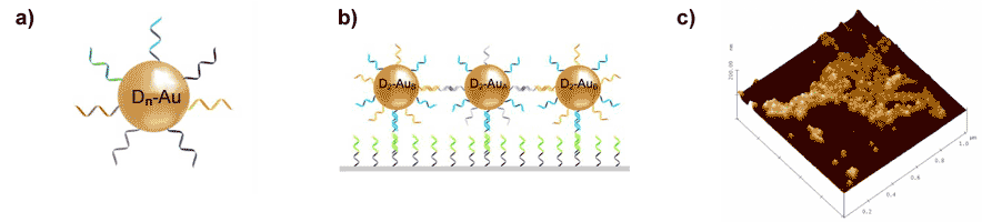
2. C.M. Niemeyer, B. Ceyhan, M. Noyong, U. Simon, Biochem. Biophys. Res. Commun. 311 (2003), 995-999.
A. Csaki, G. Maubach, D. Born, J. Reichert and W. Fritzsche: DNA-based Molecular Nanotechnology. Single Molecule 3(2002), 275-280.
A. Csaki, R. Möller, W. Straube, J.M. Köhler, W. Fritzsche: DNA monolayer on gold substrates characterized by nanoparticle labeling and scanning force microscopy. Nucleic Acids Research 29 (16) 2001, e81.
2 CNR-ISOF, Area della Ricerca, Bologna, Italy
3 Dipartimento di Fisica, Universitˆ di Modena e Reggio Emilia, Modena, Italy
In this presentation, we focus on two possible modifications: (i) G4-DNA, which is a quadruple-helical form of DNA in which adjacent stacked planes (each plane is a guanine quartet) are intercalated by metal ions; (ii) metal insertion in double-helical DNA with modified hydroxypyridone nucleobases [3]. For quadruple helical assemblies, we performed DFT-PW91 periodic-supercell calculations of infinite G4-wires [4] containing different metals (K, Ag, Cu) and discuss the results in terms of metal-guanine hybridization and expected consequences on charge mobility. We also show the different conformations (4-fold versus 8-fold coordination) that pertain to the various metals. These metal-modified DNA molecules appear under suitable conditions to be good candidates as wide-bandgap semiconductors: the metals might behave as intrinsic dopants, either by virtue of their redox activity or because of the elemental electronic configuration. For double helical assemblies, we simulated the system that was recently synthesized and characterized experimentally by Tanaka and coworkers [3]. We computed the electronic properties for a periodic wire by following their structural recipe, by means of spin-polarized DFT: We show the formation of extended orbitals with spin alignment, and compare our results to the interpretation of the EPR spectra.
[2] See discussions in the recent reviews: D. Porath, G. Cuniberti, and R. Di Felice, in Topics in Current Chemistry 237 Springer Verlag ISBN 3-540-20131-9 in press (2004); R. G. Endres, D. L. Cox, and R. R. P. Singh, Rev. Mod. Phys. 76, 195 (2004).
[3] K. Tanaka, A. Tengeiji, T. Kato, N. Toyama, and M. Shionoya, Science 299, 1212 (2003).
[4] A. Calzolari, R. Di Felice, E. Molinari, and A. Garbesi, J. Phys. Chem. B 108, 2509 (2004).
2 Department of Physics, UCSB, SB., CA.
3 Department of Chemistry, Florida State University 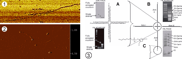
2 LPA, Ecole Normale Supérieure, 24 rue Lhomond, 75231 Paris Cedex 05, France
3 Centre de Recherche MOTOROLA Paris, MOTOROLA Labs, Espace Technologique Saint-Aubin, 91193 Gif-sur-Yvette Cedex, France 
An ideal process would be highly parallel in order to realize high throughput for both further experimental developments and possible future applications. We proposed an approach based on microstructured substrates and long DNA molecules that bind as individual molecules in an extended conformation at defined positions, and can be used for positioning of e.g. nanoparticles in further steps [1]. Utilizing micrometer-sized electrode structures and 16 µm-long DNA, a self-assembly of individual molecules on each electrode was demonstrated [2]. However, the required chemical functionalization of the electrodes and the need for a flow-chamber complicated the experiments. Utilizing the receding meniscus of a drying droplet for the extension of immobilized DNA and overlaying this process with microstructured electrode arrays, an alignment of the DNA along the electrodes could be achieved [3]. Moreover, electrode gaps were bridged by individual DNA structures by a 100% efficiency. A stepwise binding of metal nanoparticles lead to the metal nanostructures along the positioned DNA. First electrical measurements of the resulting gap structures are presented. The developed self-assembly approach presents a further step towards highly parallel processes for the precise positioning of molecular structures on chip surfaces.
2. Maubach, G.; Csaki, A.; Seidel, R.; Mertig, M.; Pompe, W.; Born, D.: Fritzsche, W. Nanotechnology 2003,14, 546-550. PDF
3. Maubach, G.: Fritzsche, W. Nano Letters 2004, 4, 607-611. PDF
The first technique takes advantage of the different electrostatic interaction between a metal AFM tip and a metal or insulating substrate. In the case of a metal tip on a conductor surface the electrostatic interaction is much higher that in the case of metal tip on a insulating substrate. According to this idea, conducting molecules should provide a stronger electrostatic interaction than insulating molecules. This a non-intrusive method that can be used to determine the electrical nature of a molecule without any electrical contact to the molecule, avoiding the problems of the electrical contact resistances. In the talk I will show different examples of electrical characterization in lambda-DNA coadsorbed with carbon nanotubes, poly(G)-Poly(C) and 4G wires.
The second method, that I will describe, is related with direct conductance measurements using AFM based techniques. In this method the molecules are partially covered with a macroscopic metal electrode that is grounded, the uncover end of the molecules are contacted by means of a gold covered AFM tip that probes the molece along its length. This method can be used to measured the current versus voltage characteristics of a molecule as a function of the tip electrode distance. In order to illustrate the method I will briefly describe experiments on single walled carbon nanotubes as a reference sample. Finally I will discuss the result of this method on 4G wires adsorbed on a mica substrate.
[2] C. M. Niemeyer, B. Ceyhan, S. Gao, L. Chi, S. Peschel, U. Simon, Colloid Polym Sci 279, 68-72 (2001).
[3] M.P.J. van Staveren, H.B. Brom, L.J. de Jongh, Physics Reports 208 (1), 1-96 (1991).
[4] V. Torma, O. Vidoni, U. Simon, G. Schmid, Eur. J. Inorg. Chem. (2003), 1121-1127
[5] U. Simon: "Electrical Properties of Nanoparticles", in G. Schmid (Ed.): "Nanoparticles: From Theory to Applications", Wiley-VCH, 2004, p. 328-367
We found conditions resulting in a highly efficient gold nanoparticle binding on the G-wire structures in combination with a low background. The assembled structure represents another versatile unit in our DNA-based toolbox for molecular construction.
2. Sondermann, A.; Holste, C.; Möller, R.; Fritzsche, W. (2002) in DNA-Based Molecular Construction pp 103-108, AIP Conference Proceedings Vol 640.
2. PRESTO, JST, Honcho 4-1-8, Kawaguchi, Saitama, Japan.
3. Department of Information Processing, Tokyo Institute of Technology, Nagatsuda 4259, Midori, Yokohama, Kanagawa 226-8502, Japan.
4. Institute of Microelectronics Technology and High Purity Materials, Russian Academy of Sciences, Chernogolovka 142432 Moscow Region, Russia.
5. Shemyakin-Ovchinnikov Institute of Bioorganic Chemistry, RAS, Miklukho-Maklaya 16/10, Moscow 117871, Russia.
6. Laboratoire de Physique des Solides, Associé au CNRS, Bât 510, Université Paris-Sud, 91405, Orsay, France.
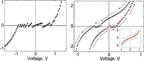
Conductivity measurements on double-stranded DNA molecules deposited by a combing process across a submicron slit between rhenium/carbon metallic contacts reveal conduction to be ohmic between room temperature and 1 kelvin. The resistance per molecule is less than 100 kilohm and varies weakly with temperature. Below the superconducting transition temperature (1 kelvin) of the contacts, proximity-induced superconductivity is observed. These results imply that DNA molecules can be conducting down to millikelvin temperature and that phase coherence is maintained over several hundred nanometers [2].
We also report the development of a new design of molecular junction, which allows the fabrication and direct visualization of a nanometer-size gap between superconducting electrodes, and also the observation and precise identification of the molecules in the gap [3]. We plan to use this technique for fabrication and study of gate controlled Josephson junctions based on DNA molecules.
2. A.Yu. Kasumov et al., Science 291, 280 (2001).
3. A.Yu. Kasumov et al., Cond-mat. 0402312.
" Nanotechnology is the technology of manipulating and constructing components and materials of nanometer size." A good example of this is the human body, whose highly advanced features are assembled from nanometer components such as DNA and proteins. Like the human body - the ultimate example of nanotechnology - all bioreactions are controlled on the atomic and molecular, or nano, level. In order to realize this concept, we have come up with the idea of " program-based self-assembly," the key word being " program." Living organisms form spontaneously - literally by themselves - out of the interactions among proteins that are synthesized by the genetic program of DNA, a blueprint with a temporal component. Using " program" as a keyword, we have developed STM imaging of DNA and related molecules, formation of DNA circuits that are constructed through programmed self-assembly. In this presentation, I will discuss following topics.
1. Bottom-up nanotechnology and DNA
2. Electronic structure of DNA: XPS, XAS, resonant photoemission, resonant Auger and Raman spectroscopy
3. Electron and hole doping; Iodine doping, electrical doping and photo-doping.
4. Polaron hopping mechanism
5. Self-assembled two dimensional network formation
6. Gold and cobalt nano-particle arrangement using programmed self-assemblyFuture DNA devices
Conductivity of native DNAs of course will depend on many factors, such as the contacts to the electrodes [1], the procedure of deposition [2]. Different types of kinks and bendings that is not resolved by using conventional Si probes can also decrease conductivity of DNAs. Images of DNA molecules obtained with these probes (Figure b) exhibit high-resolution.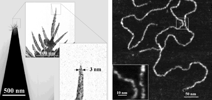
2. Kasumov A., Klinov D, Roche P.-E., Gueron S., and Bouchiat H., Applied physics letters, 84 (6), 1007-1009 (2004).
2 Dep. of Physical Chemistry, Institute of ChemistryHebrew University, Jerusalem 91904, Israel
Despite these advantages, the electrical properties of individual strands of DNA have yet to be reproducibly characterized, due to the inherent difficulties in reliably accessing and measuring single molecules. We have attacked this problem by developing protocols for reproducible formation and characterization of DNA monolayers, and then probing their electrical functioning using conducting atomic force microscopy (cAFM). The electrical contact to the DNA was made by chemical binding to a gold electrode on one end, and to a gold nanoparticle on the other. Thus, repeatable measurements of the conductivity of individual DNA strands have been performed. Meaningful differences could be detected between conductivity in single- and double-strand DNA. The single strand DNA was found to be insulating over the range of -2 to +2 V, while the double strand DNA passes significant current outside a 3 eV gap.
2- The Weizmann Institute, Rehovot, Israel,
3-Tel Aviv University, Israel
4-The University of Regensburg, Germany
We have now developed a method to attach short (26 bp) DNA molecules to a gold surface at one end and to a gold nanoparticle on the other end. Upon approaching and contacting the gold particle with a conductive AFM tip with a controlled applied force, we can measure current-voltage curves through the double-stranded DNA molecule. Preliminary measurements show relatively high currents. We report also control experiments that are performed on the insulating surrounding layer.
We also report the production and characterization of novel DNA-based molecules that may have better conduction properties.
If time allows we will report results of topography contrast inversion that is observed in STM imaging of DNA molecules (the DNA appears above the surface in parts of the image and under it in other parts). This contrast is induced either spontaneously or in a controlled way. The results are interpreted and simulated theoretically as well. 
This talk will focus on two potential applications of DPN technology. The first example illustrates the use of DPN to generate nanoscale patterns of oligonucleotides on both metallic and insulating substrates. Importantly, these patterns retain their sequence specific binding properties of the DNA of which they are composed.[3]
The second application focuses on the fabrication of sub-50-nm gold dots and line structures with deliberately designed 12-100 nm gaps. Researchers at Northwestern University initially used Dip Pen Nanolithography to pattern the etch resist, 16-mercaptohexadecanoic acid, on Au/Ti/SiOx/Si substrates and then used wet-chemical etching to remove the exposed gold.[4] In order to use these nanogaps for making electrical measurements on nanoscale matter and even molecules a pattern of thiol-modified oligonucleotides is deposited on the electrodes. In the final step DNA-functionalized nanoparticles are attached in the presence of the linking DNA strand. The current-voltage and differential conductance behaviour of the nanogap/DNA nanoparticle device is characterized at He temperatures in vacuum.
[2] D. S. Ginger, H. Zhang, C. A. Mirkin, Angew. Chem. Int. Ed. 2004, 43, 30-45
[3] L. M. Demers, D. S. Ginger, S.-J. Park, Z. Li, S.-W. Chung, C. A. Mirkin, Science 2002, 298, 1836-1838
[4] H. Zhang, S.-W. Chung, C. A. Mirkin, Nano Letters 2003, 3 (1), 43-45
Nanorobotics are key to the success of nanotechnology. To move in this direction, we have used two DX molecules to construct a DNA nanomechanical device by linking them with a segment that can be switched between left-handed Z-DNA with right-handed B-DNA. PX DNA has been used to produce a robust sequence-dependent device that changes states by varied hybridization topology. The sequence-dependent nature of this device means that a variety of them attached to a motif can all be addressed individually. Recently, we have constructed a protein-activated device that can be used to measure the ability of the protein to do work.
A central goal of DNA nanotechnology is the self-assembly of periodic matter. We have constructed micron-sized 2-dimensional DNA arrays from DX, TX and two kinds of parallelogram motifs. We can produce specific designed patterns visible in the AFM from DX and TX molecules. We can change the patterns by changing the components, and by modification after assembly. In addition, we have generated 2D arrays from DNA parallelograms. These arrays contain cavities whose sizes can be tuned by design. Recently, we have used new motifs to produce honeycomb-shaped arrays. In studies complementary to specific periodic self-assembly, we have performed algorithmic constructions, corresponding to XOR operations. Algorithmic assembly is more demanding than periodic assembly, because correct tiles are competing for their sites with partially correct tiles, rather than with incorrect tiles.
The key challenge in the area is the extension of the 2D results obtained so far to 3D systems with a high degree of ordering. Several motifs have been produced that can produce 2D arrays in each of the three directions normal to the vectors that span the 3D space. Crystals with dimensions 20-100 microns (sometimes larger) ordered to 10 Å resolution (as determined by X-ray diffraction) are relatively routine to produce. Ultimately, we expect to be able to produce high resolution crystals of DNA host lattices with heterologous guests, leading to well-ordered bio-macromolecular systems amenable to diffraction analysis. Other challenges are to incorporate DNA nanomechanical devices in periodic and aperiodic lattices and to use the lattices to organize nanoelectronic components, such as metallic nanoparticles or carbon nanotubes.
Biology contains numerous lessons for the physical sciences. The reality of living systems with nanoscale structural components represents an existence proof that autonomous systems can build up and function on this scale, systems capable of energy transduction and replication. The overall challenge that biology presents to the physical sciences is to move from biokleptic to biomimetic to abiological systems that perform in this same manner. Structural DNA nanotechnology appears to be a good place to begin to meet this challenge.
In this contribution we report on our efforts to find simple synthetic routes to chemically altered gold particles, that can be easily adopted to the synthesis in micro channel reactors. We tested two static micromixers for the direct synthesis of gold nanoparticles, starting from a gold salt solution and employing ascorbate as the reducing agent. We found, that a direct synthesis is possible in micro channels and yields particles (IPHT reactor: 15 to 18 nm; mikroglas mixer: 20 to 60 nm) comparable to those obtained on conventional routes. The mean particle diameter depends on flow rate, pH and reactand concentration. Size distributions were obtained applying an analytical disc centrifuge, that is capable of measuring size distributions of gold nanoparticles with comparable quality as ultramicroscopy. Unfortunately reactor fouling is an issue and significant deposition of particles was observed. To overcome this problem we tested kinetic controlling additives, surface treatment protocols as well as high flowrates but further experiments are needed to completely avoid adhesion of the nanoparticles to the reactors inner surfaces.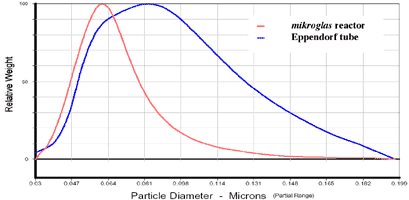
2 Advance Co.
3 Sony Corporation
If the bases of the template DNA is exposed to allow the free access of oligomers, higher yield can be expected. For this purpose, we are investigating two methods, one being the use of single-stranded DNA (ss-DNA), the other the use of recombination protein with double-stranded DNA. Electrokinetic effects are used to obtain stretch-and-positioned freely-suspended DNA in both cases. The stretching is expected to prevent entangling of the strand, formation of internal base pairs, and also to facilitate the evaluation of binding.
In the first method, fluorescence visualization of ss-DNA is realized through PCR with fluorescence-labeled dUTP added in the monomers. With the use of thus synthesized 10 kb ss-DNA, we have successfully observed its electrostatic stretching at the field strength of c.a. 3 MV/m at 1 MHz. The stretched length is about 2 µm. In comparison to 10 kbp ds-DNA, which can be stretched to the structural full length (= 3 µm) at 1 MV/m, ss-DNA requires about 3 times higher field, and still in that case, the length is about 2/3. The shorter persistent length of ss-DNA, together with still remaining internal base-pairs may explain the difference. When the electrode gap length is equal to the length of the stretched ss-DNA, dielectrophoretic collection and anchoring occurred, and ss-DNA is immobilized bridging over the adjacent electrodes.
The use of ss-DNA has disadvantage in its mechanical strength: even single defect in its backbone should result in breakage. In the second method, we use mechanically more stable ds-DNA in combination with the recombination protein RecA, which catalyzes the pairing of ss-DNA with the complementary regions on ds-DNA. When ss-DNA/RecA complex is fed to the stretch-and-positioned DNA, the sliding along, and the binding of the complex with ds-DNA is observed in single-molecule real-time basis.
We expect that these stretch-and-positioned DNA with accessible base-pairs will be a key technique to high-yield molecular construction.
This work is in part supported by the Research and Development Program for New Bio-industry Initiatives.
A method for the generation of polyaniline-polyaniline boronic acid wires on DNA was developed, and the resulting polymer wires were used to electrically contact redox-proteins with electrode surfaces.[4] The polymer wires generated on the DNA templates reveal redox functions in neutral aqueous solutions. The polymer wires were assembled on electrodes, followed by the alignment of the enzyme glucose oxidase on the wires via a surface-reconstitution process. The resulting biocatalyst was electrically-contacted with the electrode. Electrons transported to the electrode by the polymer wire enabled the bioelectrocatalyzed oxidation of glucose. In a related study,[5] chiral left or right-handed polyaniline wires were generated and assembled on electrode surfaces. The chiroselective electron transfer at the modified surfaces was demonstrated, and polymer-stimulated chiroselective bioelectrocatalysis was accomplished.
A different method to generate Au-wires on actin templates was developed, and 1.0 to 2.0 µm long Au-wires with a width of 80 nm were fabricated.[6] The wires exhibit metallic conductivity.[6] This method was also applied to construct patterned Actin-Au-wire-Actin filaments. The latter structures were used as nanotranporters and their motility on a myosin-functionalized support was followed upon addition of the ATP fuel. The gold-nanowire moves at a speed corresponding to 250 nm.s-1.
2. Y. Weizmann, F. Patolsky, I. Popov and I. Willner, Nano Lett., in press (2004).
3. Y. Weizmann and I. Willner, unpublished results.
4. L. Shi, Y. Xiao and I. Willner, submitted for publication.
5. F. Patolsky, Y. Weizmann and I. Willner, submitted for publication.

